Friday, September 5, 2014
Electronic Security Door Key Circuit Diagram
A different Electronic Security Door Key Circuit Diagram of electronic lock very simple, one and does not need a lot of materials in order to it is manufactured. The right keys of code should be stepped with the right line, so that is activated the optocupler IC2. If from error is stepped switch that does not belong in the combination, then the lock is trapped. In order to we restore the regular operation of lock, it should we press switches S1 or S12.
Read : Heat Detector Alarm using UM3561
Electronic Security Door Key Circuit Diagram
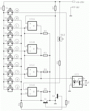
Switch S1 makes Reset of lock externally and the S12 internally, the door. The Code the circuit as he is connected it is 147 and it can change, very easily, changing the connections in the switches of keyboard. The optocupler IC2, can drive any exterior circuit as Relay etc, ensuring simultaneously electric isolation the two circuits. The circuit can be also supplied from a battery 9V.
Read : Radio Wave Alarm
Part List
R1-7-9=1Kohm
R2-3-4-5=100Kohm
R6 =10Kohm
R9 =47Kohm
IC1 = 4066
IC2 =4N25
Q1-2=BC550
S1...11=Push button sw or keyboard
S12=Push button normal closed
All resistors is 1/4W 5%

Wednesday, August 13, 2014
The Smallest Arduino Clone Possible
Everybody are making Arduino clones. So I thought I should make THE smallest. I took smallest package atmega88 – 28qfn (5mm x 5mm). Routed smallest possible resonator and as much pads as i could fit on in. The result – Smallest Arduino clone ever! Size is only 7.4mm x 7.4mm! Features include:

- Auto reset
- UART
- SPI
- 4 analog channels
- 1 digital i/o
- one LED
- funny readme with BOM
It needs arduino bootloader for atmega88 like ottantotto bootloader, probably it needs some hacking too because the resonator is 8MHz not the Arduino regular 16MHz. [Link]
Voltage Converter 0 5v to 6v Circuit Diagram
This is a Simple Voltage Converter 0.5v to 6v Circuit Diagram. Conventional silicon transistors just cant operate at voltages less than about 0.7v. Old germanium transistors could be used, but those are hard to find these days and most are rather large in size. Some new n-channel MOSFET devices with very low gate-source threshold voltage can operate at quite low voltages. Ive been experimenting with various devices and came up with one electronic circuit (shown below), which demonstrates how to boost the low voltage from a single solar cell to a higher voltage.
Voltage Converter 0.5v to 6v Circuit Diagram

The key component in the circuit below is a cheap single logic device from Texas Instruments. It turns out that TIs 74AUC family of parts can work down to about 0.45 volts. I tried one of their single schmitt trigger parts and found I was able to make on oscillator function nicely at 0.5 volts. I then used a charge pump technique and a cheap NPN transistor to form a low power flyback converter.
This hobby circuit can produce about 6 volts at the output from a 0.5v input. The idea is to use this boost circuit to generate the higher starting voltage needed by a much more powerful DC to DC converter. Once started, part of the converters output could then be feed back to the input, to sustain converter operation. This is known as a "bootstrap" technique. In the future, I hope to post a circuit which can supply several watts of power from a 0.5v input voltage. This would be ideal for charging a battery using power from a single large solar cell or several smaller cells wired in parallel.
Drown By : Dave Jhonson
Saturday, January 11, 2014
Dual Regulated Power Supply Circuit Diagram
In this circuit, the 7815 regulatates the positive supply, and the 7915 regulates the negative supply. The transformer should have a primary rating of 240/220 volts for europe, or 120 volts for North America. The centre tapped secondary coil should be rated about 18 volts at 1 amp or higher, allowing for losses in the regulator. An application for this type of circuit would be for a small regulated bench power supply.
Dual Regulated Power Supply Circuit Diagram

Friday, January 10, 2014
Tablet Reminder Uses Watch Module
This device is used as a reminder to take medicine every day. This device actually contains a crystal watch and a 4001 quad 2-input NOR gate with two of the gates (IC1a & IC1b) wired as an RS flipflop. The watch is set to "tablet time", usually mornings, when an alarm is activated with a high signal fed via diode D1 which sets the RS flipflop and enables the oscillator comprising gates IC1c & IC1d. This drives the LED with a 10% duty cycle. The 10nF capacitor resets the watch alarm when positive voltage appears on pin 3 of IC1. The circuit consumes only 50µA with a 3V battery.
Circuit diagram:

Tablet Reminder Circuit Diagram
Readmore...
Circuit diagram:

Tablet Reminder Circuit Diagram
Low Power Voltage Reference Circuit Diagram
The Low Power Voltage Reference Circuit Diagram described below, is a special implementation of current source LM334. Characterized by a very small temperature coefficient metatholio output voltage and consumes only 10uA room temperature. This current fluctuates by a few uA, when the ambient temperature varies significantly. The positive rate of temperature change LM334 offset by the negative of the contact base emitter transistors has a direct thermal coupling with the integrated.
To achieve the lowest possible temperature coefficient, it is necessary to adjust the output voltage of 1,253 V source to the arrangement easily done through R1. From the moment you get the desired output voltage, you are advised to stuck P1 and after the count value, replace it with a constant resistance. The best indeed is to replace P1 with the R1, so you have fewer parts. Prefer metal film resistors and tolerance of 1% E96 series. Having as a given that the output voltage obtained from the pin configuration LM334, is expected to show a negative resistance value 3.8 KO.
The resistance A3 ensures that the output impedance will be equal to 400 W. Under these conditions, the current that can provide the source to the load to be connected to out of retained less than 5 Ma stability of the voltage source is more than satisfactory. By varying the input voltage from 5 V to 30 V, the change in output was only 0.6 mem (from 1.2530 to 1,2536 V). The change in the thermal coefficient is maintained at values ??less than 50 ppm / C, and if you worry a bit more to the setting of the circuit, you will see that quite easily reaches 5 ppm / C. The requirements of the original circuit current was only 9.8 mA at a temperature of 22C.
Low Power Voltage Reference Circuit Diagram

Thursday, January 9, 2014
Electronic Fuse Employs A Relay
While many power supplies can be set to limit their output current to a defined level, to protect the circuit they are powering, no such protection is available if you are powering a circuit from a battery. If a fault develops, the circuit can blow before you have a chance to disconnect it. Of course, you can fit a fuse in series with the supply line to the circuit under test but it will blow if a fault develops. Or perhaps it won’t blow sufficiently quickly to protect the circuit. And repeatedly having to replace fuses becomes a nuisance as well.

The alternative is to use an electronic fuse. This circuit uses a relay to make and break the circuit. The current drain of the circuit under test is monitored by a 1O 2W resistor which is placed in series with the supply line. The voltage across this 1O resistor is monitored by op amp IC1a which has an adjustable gain of between 11 and 16, as set by trimpot VR1. The resultant DC voltage from pin 1 of IC1a is fed to pin 5 of IC1b which is configured as a comparator.
Trimpot VR2 provides an adjustable voltage reference to pin 6 of IC1b and this is compared with the amplified signal from IC1a. If IC1b’s threshold is exceeded, its pin 7 goes high and this is fed to Schmitt trigger inverter IC2a which then “sets” the RS flipflop comprising gates IC2c & IC2d. Pin 11 of IC2d then goes high to turn on transistor Q2 and LED1 while pin 4 of IC2b also goes high to turn on Q1 and the relay which then disconnects the load.
The circuit stays in this state until the RS flipflop is reset by pushing switch S1. Capacitor Cx, across the feedback resistance of IC1a, is used to simulate a slow-blow or fast-blow fuse and can be selected by trial and error. Changing the gain of IC1a or the value of the sensing resistor changes the fuse rating of the circuit.
Readmore...

The alternative is to use an electronic fuse. This circuit uses a relay to make and break the circuit. The current drain of the circuit under test is monitored by a 1O 2W resistor which is placed in series with the supply line. The voltage across this 1O resistor is monitored by op amp IC1a which has an adjustable gain of between 11 and 16, as set by trimpot VR1. The resultant DC voltage from pin 1 of IC1a is fed to pin 5 of IC1b which is configured as a comparator.
Trimpot VR2 provides an adjustable voltage reference to pin 6 of IC1b and this is compared with the amplified signal from IC1a. If IC1b’s threshold is exceeded, its pin 7 goes high and this is fed to Schmitt trigger inverter IC2a which then “sets” the RS flipflop comprising gates IC2c & IC2d. Pin 11 of IC2d then goes high to turn on transistor Q2 and LED1 while pin 4 of IC2b also goes high to turn on Q1 and the relay which then disconnects the load.
The circuit stays in this state until the RS flipflop is reset by pushing switch S1. Capacitor Cx, across the feedback resistance of IC1a, is used to simulate a slow-blow or fast-blow fuse and can be selected by trial and error. Changing the gain of IC1a or the value of the sensing resistor changes the fuse rating of the circuit.
Simple 15V And 5V Car Battery Supply Circuit Diagram
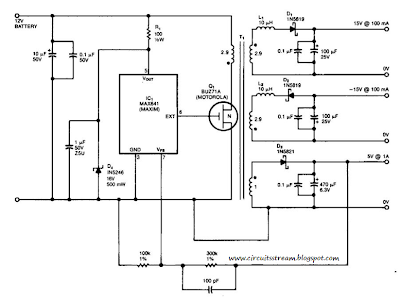
This is a Simple 15V And 5V Car Battery Supply Circuit Diagram. In this circuit use IC1 is a switching regulator that generates a 45-kHz signal that drives the gate of MOSFET Ql. Dl, D2, and D3 are Schottky diodes. The 5-V output is sensed as a reference; feedback to the chip turns off the gate signal to Ql if the voltage rises above 5 V.
Tl has Trifilar windings that assume about 2% regulation for a 10-to 100-mA load change on the ± 15-V supplies. R1/D4 provide over-voltage protection. Tl has a primary inductance of about 21 . Core size should allow 4-A peak currents. The turn ratios are IIV2 turns each for the 15-V supplies, ll1/2 turns for the primary, and four turns for the 5-V secondary. The efficiency is about 75%.
Simple 15V And 5V Car Battery Supply Circuit Diagram
Friday, December 27, 2013
Simple Tone Control by using Discrete Components
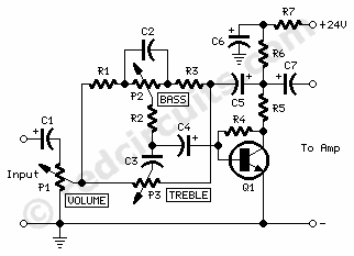
Simple Tone Control specifically designed for the 3 - 5 Watt Class-A audio amplifiers. Traditional Bass, Treble Controls and DC 24V power supply. A Bass and Treble frequency control to be added to the 3 - 5W Class-A Amplifier was required by some audio enthusiasts. Therefore, this circuit has been designed keeping in mind the extreme simplicity of the amplifier circuit to which it should be linked and was carried out using as few as components possible.
P1______________47K Log. Potentiometer (See Notes)
P2,P3___________47K Linear Potentiometers
R1,R3,R5_________4K7 1/4W Resistors
R2______________22K 1/4W Resistor
R4_______________1M 1/4W Resistor
R6_______________1K8 1/4W Resistor
R7_____________560R 1/4W Resistor
C1,C4,C5,C7_____10µF 63V Electrolytic Capacitors (See Notes)
C2______________47nF 63V Polyester Capacitor
C3_______________1nF 63V Polyester Capacitor (See Notes)
C6_____________220µF 35V Electrolytic Capacitor
Q1____________BC550 45V 100mA NPN Low noise High gain NPN Transistor
Q1 is the only active component forming a straightforward single-stage transistor amplifier with the tone control network in the ac feedback path. Taking this feedback from the split load of Q1 we obtain an ac stage gain of about 3: this can be useful to cope with low output voltage audio sources.
Readmore...
 |
| Simple Tone Control Circuit Diagram |
Parts
P1______________47K Log. Potentiometer (See Notes)
P2,P3___________47K Linear Potentiometers
R1,R3,R5_________4K7 1/4W Resistors
R2______________22K 1/4W Resistor
R4_______________1M 1/4W Resistor
R6_______________1K8 1/4W Resistor
R7_____________560R 1/4W Resistor
C1,C4,C5,C7_____10µF 63V Electrolytic Capacitors (See Notes)
C2______________47nF 63V Polyester Capacitor
C3_______________1nF 63V Polyester Capacitor (See Notes)
C6_____________220µF 35V Electrolytic Capacitor
Q1____________BC550 45V 100mA NPN Low noise High gain NPN Transistor
Q1 is the only active component forming a straightforward single-stage transistor amplifier with the tone control network in the ac feedback path. Taking this feedback from the split load of Q1 we obtain an ac stage gain of about 3: this can be useful to cope with low output voltage audio sources.
5 LED VU meter circuit diagram using KA2284
This is a simple circuit diagram of 5-LED audio VU meter using IC KA2284/KA2285. The KA2284, KA2285 are monolithic integrated circuit. It is a logarithmic display driver IC. And it is Bar type display driver using 5-Dot LED. The KA2284/KA2285 has a wide range supply voltage capacity of 3.5V-16V, but we recommend to use about a 12VDC power supply.
Circuit Diagram:
 |
| Fig: 5-LED Dot/Bar (VU meter) circuit diagram |
Usability of this circuit:
- AC signal Meter or DC Level meter.
- Audio VU(Volume Unit) meter in amplifier or such kind of device.
Here IC AN6884 is also can be used instead of KA2284,KA2285. These all are almost same.
Further reading: DOT vs BAR
Further reading: DOT vs BAR
Thursday, December 26, 2013
Reanimating Probe for AVR μC
AVR device not responding, When this discouraging message appears while you’re programming your Atmel microcontroller, that’s where the problems really begin! The problem is of ten due to incorrect programming of the fuse bits. This is where the unblocking probe comes into play.

Once the whole thing is powered up, all you have to is use one hand to apply the tip of the probe to the microcontroller’s XTAL1 input and then use your other hand to go ahead and program it with your favourite sof t ware. And there, your microcontroller is saved! The electronics are as simple as can be, the aim being to design something cheap and easy to reproduce. It consists of an oscillator generating a rectangular wave at around 500 kHz, built using a 74HC04. This circuit will also work with a 74HC14, but depending on the make of IC, the frequency of around 500 kHz may vary by around ±50 kHz. This doesn’t affect the operation of the probe.
Reanimating Probe for AVR μC Circuit diagram :

The unblocking board is connected using a ribbon cable, terminated with two female HE10/10 connectors. The pinout of the HE10/10 connector is the same as used in the majority of circuits, but of course it can be adapted for an HE10/06 connector.
The first connector is connected to the board to be unblocked, which allows powering of the electronics. The second connector is connected to the ISP programmer (STK200 compatible). The contact at the crystal is made using a needle, to ensure contact even through a board that has been varnished. There’s no need to unsolder the crystal for this operation.
The PCB design in Eagle format is available from : www.elektor.com
Author : P. Rondane - Copyright : elektor
Source :http://www.ecircuitslab.com/2012/08/reanimating-probe-for-avr-c.html
Triangular Wave Oscillator
This design resulted from the need for a partial replacement of the well-known 8038 chip, which is no longer in production and there fore hardly obtainable.
An existing design for driving an LVDT sensor (Linear Variable Differential Transformer), where the 8038 was used as a variable sine wave oscillator, had to be modernised. It may have been possible to replace the 8038 with an Exar 2206, except that this chip couldn’t be used with the supply voltage used. For this reason we looked for a replacement using standard components, which should always be available.
Triangular Wave Oscillator Circuit diagram:

In this circuit two opamps from a TL074 (IC1.A and B) are used to generate a triangular wave, which can be set to a wide range of frequencies using P1. The following differential amplifier using T1 and T2 is configured in such a way that the triangular waveform is converted into a reasonably looking sinusoidal waveform. P2 is used to adjust the distortion to a minimum.
The third opamp (IC1.C) is configured as a difference amplifier, which presents the sine wave at its output. This signal is then buffered by the last opamp (IC1.D). Any offset at the output can be nulled using P3.
Author : Jac Hettema - Copyright : Elektor
Source : http://www.ecircuitslab.com/2012/06/triangular-wave-oscillator.html
Wednesday, December 25, 2013
DIY Infrared Radar System
Chris from PyroElectro.com has a great article about a do-it-yourself radar system build with PIC18F452. It’s a great hobby project although the schematic is very complicated. This project uses three main devices to create the personal radar system. The IR Range sensor gives output, the pic microcontroller processes it and then displays the output on the led array.
DIY Infrared Radar Circuit Schematic

The goal of this project is to create a working ir radar system. The system will only be required to measure close proximity at an angle of 90 degrees as seen in the example above. The range of system is roughly 4-30cm, 20-150cm & 1m-5.5m depending upon which sensor you choose to use. [Link]DIY Infrared Radar Circuit Schematic
Telephone Conversation recorder
This circuit enables automatic switching-on of the tape recorder when the handset is lifted. The tape recorder gets switched off when the handset is replaced. The signals are suit-ably attenuated to a level at which they can be recorded using the MICIN socket of the tape recorder. Points X and Y in the circuit are connected to the telephone lines. Resistors R1 and R2 act as a voltage divider.
The voltage appearing across R2 is fed to the MIC-IN socket of the tape recorder. The values of R1 and R2 may be changed depending on the input impedance of the tape recorders MIC-IN terminals. Capacitor C1 is used for blocking the flow of DC. The second part of the circuit controls relay RL1, which is used to switch on/off the tape recorder.A voltage of 48 volts appears across the telephone lines in on-hook condition. This voltage drops to about 9 volts when the handset is lifted. Diodes D1 through D4 constitute a bridge rectifier/polarity guard.
Telephone Conversation recorder Circuit Diagram

This ensures that transistor T1 gets voltage of proper polarity, irrespective of the polarity of the telephone lines.During on-hook condition, the output from the bridge (48V DC) passes through 12V zener D5 and is applied to the base of transistor T1 via the voltage divider comprising resistors R3 and R4. This switches on transistor T1 and its collector is pulled low. This, in turn, causes transistor T2 to cut off and relay RL1 is not energised. When the telephone handset is lifted, the voltage across points X and Y falls below 12 volts and so zener diode D5 does not conduct.
As a result, base of transistor T1 is pulled to ground potential via resistor R4 and thus is cut off. Thus, base of transistor T2 gets forward biased via resistor R5, which results in the energisation of relay RL1. The tape recorder is switched on and recording begins. The tape recorder should be kept loaded with a cassette and the record button of the tape recorder should remain pressed to enable it to record the conversation as soon as the handset is lifted. Capacitor C2 ensures that the re-lay is not switched on-and-off repeatedly when a number is being dialled in pulse dialling mode.
Source: http://www.ecircuitslab.com/2011/10/telephone-conversation-recorder.html
Tuesday, December 24, 2013
LED Scanner
Here is a simple LED chaser simulating a scanner through the back and forth light effect. It used high bright White LEDs to give the chaser effect. The circuit uses an oscillator to produce fast pulses and a decade counter to drive the LEDs.
IC1 is designed as an astable multivibrator to give continuous positive pulses to the decade counter. Variable resistor VR1, R1 and C1 form the timing components. By adjusting VR1, it is possible to change the speed of the scanning LEDs.
Output pulses from IC1 are fed to the clock input of the decade counter IC2. Resistor R2 keeps the clock input of IC2 low after each positive to negative transitions of input pulses. This is necessary because sometimes the clock input of the decade counter stays positive and does not accept input pulses.
LED Scanner Circuit

All the ten outputs are used in the circuit to drive the LEDs. Diodes D1 through D10 (IN 4148) do the trick of forward and backward chasing effect. Out of the ten diodes, eight diodes form OR gates to direct the outputs of IC2 to LEDs. The remaining two diodes maintain the brightness of the two ungated LEDs. First six outputs of IC2 works in the straight way to give the running effect.
The diode connected to the pin 5 of IC2 is connected to the cathode of the diode from pin 10 (5th LED). This reverses the running sequence in the backward direction. Output 6 drives the 4th LED and the process repeats up to the 2nd LED connected to output pin2.The reset pin 15 and the Clock inhibit pin 13 of IC2 are connected to ground so that IC2 can run freely.
IC1 is designed as an astable multivibrator to give continuous positive pulses to the decade counter. Variable resistor VR1, R1 and C1 form the timing components. By adjusting VR1, it is possible to change the speed of the scanning LEDs.
Output pulses from IC1 are fed to the clock input of the decade counter IC2. Resistor R2 keeps the clock input of IC2 low after each positive to negative transitions of input pulses. This is necessary because sometimes the clock input of the decade counter stays positive and does not accept input pulses.
LED Scanner Circuit
All the ten outputs are used in the circuit to drive the LEDs. Diodes D1 through D10 (IN 4148) do the trick of forward and backward chasing effect. Out of the ten diodes, eight diodes form OR gates to direct the outputs of IC2 to LEDs. The remaining two diodes maintain the brightness of the two ungated LEDs. First six outputs of IC2 works in the straight way to give the running effect.
The diode connected to the pin 5 of IC2 is connected to the cathode of the diode from pin 10 (5th LED). This reverses the running sequence in the backward direction. Output 6 drives the 4th LED and the process repeats up to the 2nd LED connected to output pin2.The reset pin 15 and the Clock inhibit pin 13 of IC2 are connected to ground so that IC2 can run freely.
Universal Tester for 3 pin Devices
Most 3-terminal active components can be tested statically using just an ohmmeter. But when you have a lot of these devices to test, the procedure soon becomes boring. That’s where the idea came from to combine fast, easy testing for these types of device into a single instrument.
The unit described here enables you to test NPN and PNP bipolar transistors, N-or Pchannel FETs or MOSFETs, UJTs, triacs, and thyristors. Regardless of the type of device, the tests are non-destructive. Universal connectors allow testing of all package types, including SMDs (up to a point). The unit lets you change from one type of device to another in a trice. It avoids using a multi-pole switch, as they’re too expensive and hard to find.

Here’s how to build a versatile instrument at a ridiculously low cost. IC1 is a 4066 quad CMOS switch which will let us switch between bipolar transistors and FETs. LEDs D1–D4 tell us about the condition of the test device, when we press the ‘Test’ button. The 4066 can only handle a few milliamps, not enough for the other component types to be tested, hence the reason for using relay RE1. This 12 V relay offers two NO contacts. The first applies power to the UJT test circuit, the second applies it to the triac and thyristor test circuit.
Extensive testing has shown that the best way to test UJT transistors is to do so dynamically, with the help of a relaxation oscillator. Net-work R11/C1 sets the oscillator frequency to around 2 Hz. On pin B1 of the UJT we find a nice sawtooth, which is not of much interest to us here. However, pin B2 gives good but very short pulses. IC2, wired as a monostable, lengthens these pulses so they can be clearly seen via LED D5.
The relay’s second pole is going to drive the thyristor’ sortriac’s trigger pin. The value of R18 is a good compromise with respect to the varying trigger currents for this type of device. Resistor R17 is important, as the hold-ing current must be high enough for a triac; 250 mA is a good compromise. LED D6 tells you if the device is in good condition or not; but watch out, the test result must be con-firmed by briefly cutting the power in order to reset the triac.
On the web page for this article [1] you’ll find the author’s CAD files (PCB layout and front panel) along with some photos of his project. On the prototype, the LEDs and the ‘Test’ button were wired onto the copper side of the PCB. The six female connectors for the devices being tested were salvaged, but there are lots of models available on the market (the pitch is standard). The test cable crocodile clips must be as small as possible for testing SMD devices.
Source : http://www.ecircuitslab.com/2012/05/universal-tester-for-3-pin-devices.html
Monday, December 23, 2013
3 Rail Power supply Circuit Diagram
This 3- Rail Power supply Circuit Diagram generates three supply voltages using a minimum of components. Diodes D2 and D3 perform full-wave rectification, alternately charging capacitor C2 on both halves of the ac cycle. On the other hand, diode D1 with capacitor C1, and diode D4 with capacitor C3 each perform half-wave rectification.
The full-and half-wave rectification arrangement is satisfactory for modest supply currents drawn from -5 and +12-V regulators IC3 and IC2. You can use this circuit as an auxiliary supply in an up-based instrument, for example, and avoid the less attractive alternatives of buying a custom-wound transformer, building a more complex supply, or using a secondary winding, say 18 Vac, and wasting power in the 5-V regulators.
3- Rail Power supply Circuit Diagram

12KV High Voltage Generator
The hobby circuit below uses an unusual method to generate about 12,000 volts with about 5uA of current. Two SCRs form two pulse generator circuits. The two SCRs discharge a 0.047uF a 400v capacitor through a xenon lamp trigger coil at 120 times a second. The high voltage pulses produced at the secondary of the trigger coil are rectified using two 6KV damper diodes.

The voltage doubler circuit at the secondary of the trigger coil charges up two high voltage disc capacitors up to about 12KV. Although this circuit can’t produce a lot of current be very careful with it. A 12KV spark can jump about 0.75 of an inch so the electronic circuit needs to be carefully wired with lots of space between components.
Readmore...
The voltage doubler circuit at the secondary of the trigger coil charges up two high voltage disc capacitors up to about 12KV. Although this circuit can’t produce a lot of current be very careful with it. A 12KV spark can jump about 0.75 of an inch so the electronic circuit needs to be carefully wired with lots of space between components.
Sunday, December 22, 2013
Easy Dc To Dc Converter Circuit Diagram
This Easy Dc To Dc Converter Circuit Diagram uses a Linear Technology LT1073 in a -24-V converter. The supply can be two AA cells (3 V) or 5 V. The circuit can deliver 7 mA.
Dc To Dc Converter Circuit Diagram

Dc To Dc Converter Circuit Diagram
1000 watt power inverter circuit diagram
This 1000 watt power inverter circuit diagram based on MOSFET RF50N06.If you want more power then add additional MOSFET paralleled at RF50N06.This MOSFETS are 60 Volts and 50 Amps as rated. It is necessary to connect a FUSE with the power line and always a LOAD have to connected while power is being applied . The output power of this inverter is up-to 1k watt , it depends on output power transformer . You can use your custom transformer with experimenting for best result.
Circuit Diagram | 1000 watt power inverter
 |
| Fig:Schematic diagram of 1000 watt power inverter |
How to parallel MOSFETs | 1000 watt power inverter

Source: http://www3.telus.net/chemelec/Projects/Inverter/Mosfet-Inverter.htm
Subscribe to:
Posts (Atom)