Showing posts with label simple. Show all posts
Showing posts with label simple. Show all posts
Thursday, January 9, 2014
Simple 15V And 5V Car Battery Supply Circuit Diagram
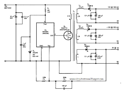
This is a Simple 15V And 5V Car Battery Supply Circuit Diagram. In this circuit use IC1 is a switching regulator that generates a 45-kHz signal that drives the gate of MOSFET Ql. Dl, D2, and D3 are Schottky diodes. The 5-V output is sensed as a reference; feedback to the chip turns off the gate signal to Ql if the voltage rises above 5 V.
Tl has Trifilar windings that assume about 2% regulation for a 10-to 100-mA load change on the ± 15-V supplies. R1/D4 provide over-voltage protection. Tl has a primary inductance of about 21 . Core size should allow 4-A peak currents. The turn ratios are IIV2 turns each for the 15-V supplies, ll1/2 turns for the primary, and four turns for the 5-V secondary. The efficiency is about 75%.
Simple 15V And 5V Car Battery Supply Circuit Diagram

Friday, December 27, 2013
Simple Tone Control by using Discrete Components
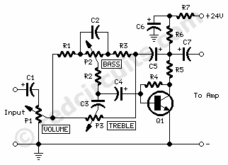
Simple Tone Control specifically designed for the 3 - 5 Watt Class-A audio amplifiers. Traditional Bass, Treble Controls and DC 24V power supply. A Bass and Treble frequency control to be added to the 3 - 5W Class-A Amplifier was required by some audio enthusiasts. Therefore, this circuit has been designed keeping in mind the extreme simplicity of the amplifier circuit to which it should be linked and was carried out using as few as components possible.
P1______________47K Log. Potentiometer (See Notes)
P2,P3___________47K Linear Potentiometers
R1,R3,R5_________4K7 1/4W Resistors
R2______________22K 1/4W Resistor
R4_______________1M 1/4W Resistor
R6_______________1K8 1/4W Resistor
R7_____________560R 1/4W Resistor
C1,C4,C5,C7_____10µF 63V Electrolytic Capacitors (See Notes)
C2______________47nF 63V Polyester Capacitor
C3_______________1nF 63V Polyester Capacitor (See Notes)
C6_____________220µF 35V Electrolytic Capacitor
Q1____________BC550 45V 100mA NPN Low noise High gain NPN Transistor
Q1 is the only active component forming a straightforward single-stage transistor amplifier with the tone control network in the ac feedback path. Taking this feedback from the split load of Q1 we obtain an ac stage gain of about 3: this can be useful to cope with low output voltage audio sources.
Readmore...
 |
| Simple Tone Control Circuit Diagram |
Parts
P1______________47K Log. Potentiometer (See Notes)
P2,P3___________47K Linear Potentiometers
R1,R3,R5_________4K7 1/4W Resistors
R2______________22K 1/4W Resistor
R4_______________1M 1/4W Resistor
R6_______________1K8 1/4W Resistor
R7_____________560R 1/4W Resistor
C1,C4,C5,C7_____10µF 63V Electrolytic Capacitors (See Notes)
C2______________47nF 63V Polyester Capacitor
C3_______________1nF 63V Polyester Capacitor (See Notes)
C6_____________220µF 35V Electrolytic Capacitor
Q1____________BC550 45V 100mA NPN Low noise High gain NPN Transistor
Q1 is the only active component forming a straightforward single-stage transistor amplifier with the tone control network in the ac feedback path. Taking this feedback from the split load of Q1 we obtain an ac stage gain of about 3: this can be useful to cope with low output voltage audio sources.
Monday, December 16, 2013
Simple Battery charger Circuit Diagram
This is a simple Battery charger circuit diagram. A diac is used in the gate circuit to provide work for the signal being applied to the gate. R1 a threshold level for firing the triac. C3 and R4 is selected to limit the maximum charging cur-provide a transient suppression network Rl, rent at full Totation of R2. R2, R3, Cl, and C2 provide a phase-shift net.
Simple Battery charger Circuit Diagram

Simple Battery charger Circuit Diagram
Monday, October 7, 2013
Simple MD Catridge Preamplifier
Phonographs are gradually becoming a rarity. Most of them have had to yield to more advanced systems, such as CD players and recorders or (portable) MiniDisc player/recorders. This trend is recognized by manufacturers of audio installations, which means that the traditional phono input is missing on increasingly more systems. Hi-fi enthusiasts who want make digital versions of their existing collections of phonograph records on a CD or MD, discover that it is no longer possible to connect a phonograph to the system.
 However, with a limited amount of circuitry, it is possible to adapt the line input of a modern amplifier or recorder so that it can handle the low-level signals generated by the magnetodynamic cartridge of a phonograph. Of course, the circuit has to provide the well-known RIAA correction that must be used with these cartridges. The preamplifier shown here performs the job using only one opamp, four resistors and four capacitors. For a stereo version, you will naturally need two of everything. Any stabilized power supply that can deliver ±15V can be used as a power source.
Readmore...
 However, with a limited amount of circuitry, it is possible to adapt the line input of a modern amplifier or recorder so that it can handle the low-level signals generated by the magnetodynamic cartridge of a phonograph. Of course, the circuit has to provide the well-known RIAA correction that must be used with these cartridges. The preamplifier shown here performs the job using only one opamp, four resistors and four capacitors. For a stereo version, you will naturally need two of everything. Any stabilized power supply that can deliver ±15V can be used as a power source.
Sunday, October 6, 2013
Simple Battery Charger Circuit Charges Upto 12 NiCD Cells
This handy circuit can be used to charge from one to 12 NiCd cells from a car battery. Up to six cells can be charged with switch S1 in the "normal" position. The LM317regulator operates as a simple current source, providing about 530mA when R1 = 2.35O (two 4.7O resistors in parallel). For more than six cells, S1 is set to the "boost" position. This applies powers to IC1, a 10W (or 20W) audio power amplifier. Positive feedback from its output (pin 4) to non-inverting input (pin 1) causes IC1 to act as a square wave oscillator. This square wave signal is coupled to the junction of Schottky diodes D1 and D2 via a 330µF capacitor, forming a conventional charge-pump voltage doubler. Over 20V (unloaded) appears at the input to REG1 - enough to charge a maximum of 12 cells!

Readmore...

Monday, September 30, 2013
Simple But Reliable Car Battery Tester
This circuit uses the popular and easy to find LM3914 IC. This IC is very simple to drive, needs no voltage regulators (it has a built in voltage regulator) and can be powered from almost every source. This circuit is very easy to explain: When the test button is pressed, the Car battery voltage is feed into a high impedance voltage divider. His purpose is to divide 12V to 1,25V (or lower values to lower values).
This solution is better than letting the internal voltage regulator set the 12V sample voltage to be feed into the internal voltage divider simply because it cannot regulate 12V when the voltage drops lower (linear regulators only step down). Simply wiring with no adjust, the regulator provides stable 1,25V which is fed into the precision internal resistor cascade to generate sample voltages for the internal comparators. Anyway the default setting let you to measure voltages between 8 and 12V but you can measure even from 0V to 12V setting the offset trimmer to 0 (but i think that under 9 volt your car would not start).

There is a smoothing capacitor (4700uF 16V) it is used to adsorb EMF noise produced from the ignition coil if you are measuring the battery during the engine working. Diesel engines would not need it, but Im not sure. If you like more a point graph rather than a bar graph simply disconnect pin 9 on the IC (MODE) from power. The calculations are simple (default)
For the first comparator the voltage is : 0,833 V corresponding to 8 V
* * * * * voltage is : 0,875 V corresponding to 8,4 V
for the last comparator the voltage is : 1,25 V corresponding to 12 V
Have fun, learn and dont let you car battery discharge... ;-)
This solution is better than letting the internal voltage regulator set the 12V sample voltage to be feed into the internal voltage divider simply because it cannot regulate 12V when the voltage drops lower (linear regulators only step down). Simply wiring with no adjust, the regulator provides stable 1,25V which is fed into the precision internal resistor cascade to generate sample voltages for the internal comparators. Anyway the default setting let you to measure voltages between 8 and 12V but you can measure even from 0V to 12V setting the offset trimmer to 0 (but i think that under 9 volt your car would not start).
There is a smoothing capacitor (4700uF 16V) it is used to adsorb EMF noise produced from the ignition coil if you are measuring the battery during the engine working. Diesel engines would not need it, but Im not sure. If you like more a point graph rather than a bar graph simply disconnect pin 9 on the IC (MODE) from power. The calculations are simple (default)
For the first comparator the voltage is : 0,833 V corresponding to 8 V
* * * * * voltage is : 0,875 V corresponding to 8,4 V
for the last comparator the voltage is : 1,25 V corresponding to 12 V
Have fun, learn and dont let you car battery discharge... ;-)
author: Jonathan Filippi
e-mail: jonathan.filippi@virgilio.it
e-mail: jonathan.filippi@virgilio.it
Sunday, September 1, 2013
Simple Analog to Digital Converter
Normally analogue-to-digital con-verter (ADC) needs interfacing through a microprocessor to convert analogue data into digital format. This requires hardware and necessary software, resulting in increased complexity and hence the total cost.
The circuit of A-to-D converter shown here is configured around ADC 0808, avoiding the use of a microprocessor. The ADC 0808 is an 8-bit A-to-D converter, having data lines D0-D7. It works on the principle of successive approximation. It has a total of eight analogue input channels, out of which any one can be selected using address lines A, B and C. Here, in this case, input channel IN0 is selected by grounding A, B and C address lines.
Simple Analog to Digital Converter Circuit diagram

Usually the control signals EOC (end of conversion), SC (start conversion), ALE (address latch enable) and OE (output enable) are interfaced by means of a microprocessor. However, the circuit shown here is built to operate in its continuous mode without using any microprocessor. Therefore the input control signals ALE and OE, being active-high, are tied to Vcc (+5 volts). The input control signal SC, being active-low, initiates start of conversion at falling edge of the pulse, whereas the output signal EOC becomes high after completion of digitisation. This EOC output is coupled to SC input, where falling edge of EOC output acts as SC input to direct the ADC to start the conversion.
As the conversion starts, EOC signal goes high. At next clock pulse EOC output again goes low, and hence SC is enabled to start the next conversion. Thus, it provides continuous 8-bit digital output corresponding to instantaneous value of analogue input. The maximum level of analogue input voltage should be appropriately scaled down below positive reference (+5V) level.
The ADC 0808 IC requires clock signal of typically 550 kHz, which can be easily derived from an astable multivibrator constructed using 7404 inverter gates. In order to visualise the digital output, the row of eight LEDs (LED1 through LED8) have been used, wherein each LED is connected to respective data lines D0 through D7. Since ADC works in the continuous mode, it displays digital output as soon as analogue input is applied. The decimal equivalent digital output value D for a given analogue input voltage Vin can be calculated from the relationship
The circuit of A-to-D converter shown here is configured around ADC 0808, avoiding the use of a microprocessor. The ADC 0808 is an 8-bit A-to-D converter, having data lines D0-D7. It works on the principle of successive approximation. It has a total of eight analogue input channels, out of which any one can be selected using address lines A, B and C. Here, in this case, input channel IN0 is selected by grounding A, B and C address lines.
Simple Analog to Digital Converter Circuit diagram

Usually the control signals EOC (end of conversion), SC (start conversion), ALE (address latch enable) and OE (output enable) are interfaced by means of a microprocessor. However, the circuit shown here is built to operate in its continuous mode without using any microprocessor. Therefore the input control signals ALE and OE, being active-high, are tied to Vcc (+5 volts). The input control signal SC, being active-low, initiates start of conversion at falling edge of the pulse, whereas the output signal EOC becomes high after completion of digitisation. This EOC output is coupled to SC input, where falling edge of EOC output acts as SC input to direct the ADC to start the conversion.
As the conversion starts, EOC signal goes high. At next clock pulse EOC output again goes low, and hence SC is enabled to start the next conversion. Thus, it provides continuous 8-bit digital output corresponding to instantaneous value of analogue input. The maximum level of analogue input voltage should be appropriately scaled down below positive reference (+5V) level.
The ADC 0808 IC requires clock signal of typically 550 kHz, which can be easily derived from an astable multivibrator constructed using 7404 inverter gates. In order to visualise the digital output, the row of eight LEDs (LED1 through LED8) have been used, wherein each LED is connected to respective data lines D0 through D7. Since ADC works in the continuous mode, it displays digital output as soon as analogue input is applied. The decimal equivalent digital output value D for a given analogue input voltage Vin can be calculated from the relationship
Friday, August 30, 2013
Simple SWR and PWR Meter
Many SWR / Power meter used by amateurs to the extent reasonably accurate continuous average power with a CW key-down signal, but can not reliably be used with other (modulated) signals PEP or average power measurement. These laws seek to show why the power measurement can be a sensitive issue, and because the interpretation of a yardstick of power can be a lot of attention and knowledge of construction and the characteristics of the instrument.
A reflectometer-type SWR meter can be calibrated to give power back and forth (PF, Pr) on a power supply. A classic example is the 1943 Bird Series power meter, which is a directional coupler is used to obtain a sample voltage proportional to the voltage wave or forward or backward on the feeder (VF, VR). Other systems, perhaps more suitable for HF, then use a bridge circuit to perform the same function.
Simple SWR and PWR Meter Circuit diagram
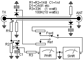
The sample voltage is then rectified and displayed on a meter that is calibrated in watts. If the counter is typically a coil, the scale, so the numbers on the scale, representing the power, are proportional to the square of the applied voltage or the current calibration. The theory of this type is very simple and is based on the concept represented by PF = Vf2/Zo. Note that if the power supply has an impedance that differs from the value of how the instrument is calibrated, there will be a mistake. The output voltage of the rectifier is a solid phase of VF or VR, and this is expected in the calibration of the meter.
Examples of directional coupling, and bridge-type reflectometers are shown in Figures 1 and 2, while the bird directional coupler means 43 is illustrated in Figure 3. Note that in all cases the measurement circuit, a combination with a small RC time constant, making the system unsuitable for the measurement of PEP, and the absence of a specific device quadratic, making them unsuitable for measuring the average power .
A reflectometer-type SWR meter can be calibrated to give power back and forth (PF, Pr) on a power supply. A classic example is the 1943 Bird Series power meter, which is a directional coupler is used to obtain a sample voltage proportional to the voltage wave or forward or backward on the feeder (VF, VR). Other systems, perhaps more suitable for HF, then use a bridge circuit to perform the same function.
Simple SWR and PWR Meter Circuit diagram
The sample voltage is then rectified and displayed on a meter that is calibrated in watts. If the counter is typically a coil, the scale, so the numbers on the scale, representing the power, are proportional to the square of the applied voltage or the current calibration. The theory of this type is very simple and is based on the concept represented by PF = Vf2/Zo. Note that if the power supply has an impedance that differs from the value of how the instrument is calibrated, there will be a mistake. The output voltage of the rectifier is a solid phase of VF or VR, and this is expected in the calibration of the meter.
Examples of directional coupling, and bridge-type reflectometers are shown in Figures 1 and 2, while the bird directional coupler means 43 is illustrated in Figure 3. Note that in all cases the measurement circuit, a combination with a small RC time constant, making the system unsuitable for the measurement of PEP, and the absence of a specific device quadratic, making them unsuitable for measuring the average power .
Subscribe to:
Posts (Atom)