Friday, September 5, 2014
Electronic Security Door Key Circuit Diagram
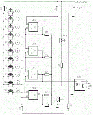
A different Electronic Security Door Key Circuit Diagram of electronic lock very simple, one and does not need a lot of materials in order to it is manufactured. The right keys of code should be stepped with the right line, so that is activated the optocupler IC2. If from error is stepped switch that does not belong in the combination, then the lock is trapped. In order to we restore the regular operation of lock, it should we press switches S1 or S12.
Read : Heat Detector Alarm using UM3561
Electronic Security Door Key Circuit Diagram

Switch S1 makes Reset of lock externally and the S12 internally, the door. The Code the circuit as he is connected it is 147 and it can change, very easily, changing the connections in the switches of keyboard. The optocupler IC2, can drive any exterior circuit as Relay etc, ensuring simultaneously electric isolation the two circuits. The circuit can be also supplied from a battery 9V.
Read : Radio Wave Alarm
Part List
R1-7-9=1Kohm
R2-3-4-5=100Kohm
R6 =10Kohm
R9 =47Kohm
IC1 = 4066
IC2 =4N25
Q1-2=BC550
S1...11=Push button sw or keyboard
S12=Push button normal closed
All resistors is 1/4W 5%
Wednesday, August 13, 2014
The Smallest Arduino Clone Possible
Everybody are making Arduino clones. So I thought I should make THE smallest. I took smallest package atmega88 – 28qfn (5mm x 5mm). Routed smallest possible resonator and as much pads as i could fit on in. The result – Smallest Arduino clone ever! Size is only 7.4mm x 7.4mm! Features include:

- Auto reset
- UART
- SPI
- 4 analog channels
- 1 digital i/o
- one LED
- funny readme with BOM
It needs arduino bootloader for atmega88 like ottantotto bootloader, probably it needs some hacking too because the resonator is 8MHz not the Arduino regular 16MHz. [Link]
Voltage Converter 0 5v to 6v Circuit Diagram
This is a Simple Voltage Converter 0.5v to 6v Circuit Diagram. Conventional silicon transistors just cant operate at voltages less than about 0.7v. Old germanium transistors could be used, but those are hard to find these days and most are rather large in size. Some new n-channel MOSFET devices with very low gate-source threshold voltage can operate at quite low voltages. Ive been experimenting with various devices and came up with one electronic circuit (shown below), which demonstrates how to boost the low voltage from a single solar cell to a higher voltage.
Voltage Converter 0.5v to 6v Circuit Diagram

The key component in the circuit below is a cheap single logic device from Texas Instruments. It turns out that TIs 74AUC family of parts can work down to about 0.45 volts. I tried one of their single schmitt trigger parts and found I was able to make on oscillator function nicely at 0.5 volts. I then used a charge pump technique and a cheap NPN transistor to form a low power flyback converter.
This hobby circuit can produce about 6 volts at the output from a 0.5v input. The idea is to use this boost circuit to generate the higher starting voltage needed by a much more powerful DC to DC converter. Once started, part of the converters output could then be feed back to the input, to sustain converter operation. This is known as a "bootstrap" technique. In the future, I hope to post a circuit which can supply several watts of power from a 0.5v input voltage. This would be ideal for charging a battery using power from a single large solar cell or several smaller cells wired in parallel.
Drown By : Dave Jhonson
Saturday, January 11, 2014
Dual Regulated Power Supply Circuit Diagram
In this circuit, the 7815 regulatates the positive supply, and the 7915 regulates the negative supply. The transformer should have a primary rating of 240/220 volts for europe, or 120 volts for North America. The centre tapped secondary coil should be rated about 18 volts at 1 amp or higher, allowing for losses in the regulator. An application for this type of circuit would be for a small regulated bench power supply.
Dual Regulated Power Supply Circuit Diagram

Friday, January 10, 2014
Tablet Reminder Uses Watch Module
This device is used as a reminder to take medicine every day. This device actually contains a crystal watch and a 4001 quad 2-input NOR gate with two of the gates (IC1a & IC1b) wired as an RS flipflop. The watch is set to "tablet time", usually mornings, when an alarm is activated with a high signal fed via diode D1 which sets the RS flipflop and enables the oscillator comprising gates IC1c & IC1d. This drives the LED with a 10% duty cycle. The 10nF capacitor resets the watch alarm when positive voltage appears on pin 3 of IC1. The circuit consumes only 50µA with a 3V battery.
Circuit diagram:

Tablet Reminder Circuit Diagram
Readmore...
Circuit diagram:

Tablet Reminder Circuit Diagram
Low Power Voltage Reference Circuit Diagram
The Low Power Voltage Reference Circuit Diagram described below, is a special implementation of current source LM334. Characterized by a very small temperature coefficient metatholio output voltage and consumes only 10uA room temperature. This current fluctuates by a few uA, when the ambient temperature varies significantly. The positive rate of temperature change LM334 offset by the negative of the contact base emitter transistors has a direct thermal coupling with the integrated.
To achieve the lowest possible temperature coefficient, it is necessary to adjust the output voltage of 1,253 V source to the arrangement easily done through R1. From the moment you get the desired output voltage, you are advised to stuck P1 and after the count value, replace it with a constant resistance. The best indeed is to replace P1 with the R1, so you have fewer parts. Prefer metal film resistors and tolerance of 1% E96 series. Having as a given that the output voltage obtained from the pin configuration LM334, is expected to show a negative resistance value 3.8 KO.
The resistance A3 ensures that the output impedance will be equal to 400 W. Under these conditions, the current that can provide the source to the load to be connected to out of retained less than 5 Ma stability of the voltage source is more than satisfactory. By varying the input voltage from 5 V to 30 V, the change in output was only 0.6 mem (from 1.2530 to 1,2536 V). The change in the thermal coefficient is maintained at values ??less than 50 ppm / C, and if you worry a bit more to the setting of the circuit, you will see that quite easily reaches 5 ppm / C. The requirements of the original circuit current was only 9.8 mA at a temperature of 22C.
Low Power Voltage Reference Circuit Diagram

Thursday, January 9, 2014
Electronic Fuse Employs A Relay
While many power supplies can be set to limit their output current to a defined level, to protect the circuit they are powering, no such protection is available if you are powering a circuit from a battery. If a fault develops, the circuit can blow before you have a chance to disconnect it. Of course, you can fit a fuse in series with the supply line to the circuit under test but it will blow if a fault develops. Or perhaps it won’t blow sufficiently quickly to protect the circuit. And repeatedly having to replace fuses becomes a nuisance as well.

The alternative is to use an electronic fuse. This circuit uses a relay to make and break the circuit. The current drain of the circuit under test is monitored by a 1O 2W resistor which is placed in series with the supply line. The voltage across this 1O resistor is monitored by op amp IC1a which has an adjustable gain of between 11 and 16, as set by trimpot VR1. The resultant DC voltage from pin 1 of IC1a is fed to pin 5 of IC1b which is configured as a comparator.
Trimpot VR2 provides an adjustable voltage reference to pin 6 of IC1b and this is compared with the amplified signal from IC1a. If IC1b’s threshold is exceeded, its pin 7 goes high and this is fed to Schmitt trigger inverter IC2a which then “sets” the RS flipflop comprising gates IC2c & IC2d. Pin 11 of IC2d then goes high to turn on transistor Q2 and LED1 while pin 4 of IC2b also goes high to turn on Q1 and the relay which then disconnects the load.
The circuit stays in this state until the RS flipflop is reset by pushing switch S1. Capacitor Cx, across the feedback resistance of IC1a, is used to simulate a slow-blow or fast-blow fuse and can be selected by trial and error. Changing the gain of IC1a or the value of the sensing resistor changes the fuse rating of the circuit.
Readmore...

The alternative is to use an electronic fuse. This circuit uses a relay to make and break the circuit. The current drain of the circuit under test is monitored by a 1O 2W resistor which is placed in series with the supply line. The voltage across this 1O resistor is monitored by op amp IC1a which has an adjustable gain of between 11 and 16, as set by trimpot VR1. The resultant DC voltage from pin 1 of IC1a is fed to pin 5 of IC1b which is configured as a comparator.
Trimpot VR2 provides an adjustable voltage reference to pin 6 of IC1b and this is compared with the amplified signal from IC1a. If IC1b’s threshold is exceeded, its pin 7 goes high and this is fed to Schmitt trigger inverter IC2a which then “sets” the RS flipflop comprising gates IC2c & IC2d. Pin 11 of IC2d then goes high to turn on transistor Q2 and LED1 while pin 4 of IC2b also goes high to turn on Q1 and the relay which then disconnects the load.
The circuit stays in this state until the RS flipflop is reset by pushing switch S1. Capacitor Cx, across the feedback resistance of IC1a, is used to simulate a slow-blow or fast-blow fuse and can be selected by trial and error. Changing the gain of IC1a or the value of the sensing resistor changes the fuse rating of the circuit.
Simple 15V And 5V Car Battery Supply Circuit Diagram
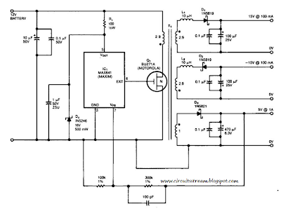
This is a Simple 15V And 5V Car Battery Supply Circuit Diagram. In this circuit use IC1 is a switching regulator that generates a 45-kHz signal that drives the gate of MOSFET Ql. Dl, D2, and D3 are Schottky diodes. The 5-V output is sensed as a reference; feedback to the chip turns off the gate signal to Ql if the voltage rises above 5 V.
Tl has Trifilar windings that assume about 2% regulation for a 10-to 100-mA load change on the ± 15-V supplies. R1/D4 provide over-voltage protection. Tl has a primary inductance of about 21 . Core size should allow 4-A peak currents. The turn ratios are IIV2 turns each for the 15-V supplies, ll1/2 turns for the primary, and four turns for the 5-V secondary. The efficiency is about 75%.
Simple 15V And 5V Car Battery Supply Circuit Diagram

Subscribe to:
Comments (Atom)