Friday, September 5, 2014
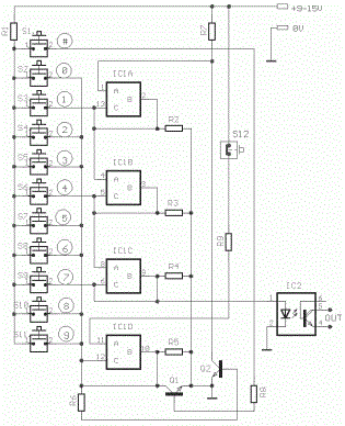
Electronic Security Door Key Circuit Diagram

Part List
R1-7-9=1Kohm
R2-3-4-5=100Kohm
R6 =10Kohm
R9 =47Kohm
IC1 = 4066
IC2 =4N25
Q1-2=BC550
S1...11=Push button sw or keyboard
S12=Push button normal closed
All resistors is 1/4W 5%
Wednesday, August 13, 2014
Voltage Converter 0 5v to 6v Circuit Diagram

Saturday, January 11, 2014
Dual Regulated Power Supply Circuit Diagram

Friday, January 10, 2014
Low Power Voltage Reference Circuit Diagram

Thursday, January 9, 2014
Simple 15V And 5V Car Battery Supply Circuit Diagram

Friday, December 27, 2013
5 LED VU meter circuit diagram using KA2284
Circuit Diagram:
 |
| Fig: 5-LED Dot/Bar (VU meter) circuit diagram |
Usability of this circuit:
- AC signal Meter or DC Level meter.
- Audio VU(Volume Unit) meter in amplifier or such kind of device.
Further reading: DOT vs BAR
Monday, December 23, 2013
3 Rail Power supply Circuit Diagram

Sunday, December 22, 2013
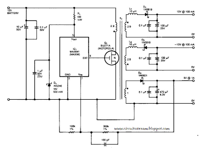
Easy Dc To Dc Converter Circuit Diagram
Dc To Dc Converter Circuit Diagram

1000 watt power inverter circuit diagram
Circuit Diagram | 1000 watt power inverter
 |
| Fig:Schematic diagram of 1000 watt power inverter |
How to parallel MOSFETs | 1000 watt power inverter

Source: http://www3.telus.net/chemelec/Projects/Inverter/Mosfet-Inverter.htm
Friday, December 20, 2013
Warning Light and Marker Light Circuit Diagram
Warning Light and Marker Light Circuit Diagram

Monday, December 16, 2013
Simple Battery charger Circuit Diagram

Wednesday, October 9, 2013
Li Ion Battery Charger Circuit
The LP2951 regulator is manufactured by National Semiconductors. The choice of values is from an application note "Battery Charging", written by Chester Simpson. Diode D1 can be any diode from the 1N00x series, whichever is conveniently available. It functions as a blocking diode, to prevent a back flow of current from the battery into the LP2951 when the input voltage is disconnected. Charging current is about 100+mA, which is the internally-limited maximum current of the LP2951. For those wondering, this is compatible with just about any single-cell li-ion battery since li-ion can generally accept a charging current of up to about 1c (i.e. charging current in mA equivalent to their capacity in mAh, so a 1100mAh li-ion cell can be charged at up to 1100mA and so on).
Circuit diagram:
 Li-Ion Battery Charger Circuit diagram
A lower charging current just brings about a correspondingly longer charge time. IMHO 100mA is quite low, low enough that the circuit can be used for an overnight charger for many typical single-cell li-ion batteries. The resistors are deliberately kept at large orders of magnitude (tens/hundred Kohm and Mohm range) to keep the off-state current as low as possible, at about 2?A. Resistor tolerances should be kept at 1% for output voltage accuracy. The 50k pot allows for an output voltage range between 4.08V to 4.26V - thus allowing calibration as well as a choice between a charging voltage of 4.1V or 4.2V depending on the cell to be charged. The capacitors are for stability, especially C2 which prevents the output from ringing/oscillating.
Parts
IC1 = LP2951, voltage regulator
D1 = 1N4002, General purpose diode
R1 = 2M, 1%, metal-film
R2 = 806K, 1%, metal-film
P1 = 50K, potentiometer
C1 = 0.1uF, polyester
C2 = 2.2uF/16V, electrolytic
C3 = 330pF, ceramic
Source :www.extremecircuits.net
Sunday, October 6, 2013
Simple Battery Charger Circuit Charges Upto 12 NiCD Cells
Friday, October 4, 2013
Lead Acid Battery Charger Circuit 2
The above pictured schematic diagram is just a standard constant current model with a added current limiter, consisting of Q1, R1, and R4. The moment too much current is flowing biases Q1 and drops the output voltage. The output voltage is: 1.2 x (P1+R2+R3)/R3 volt. Current limiting kicks in when the current is about 0.6/R1 amp. For a 6-volt battery which requires fast-charging, the charge voltage is 3 x 2.45 = 7.35 V. (3 cells at 2.45v per cell).
So the total value for R2 + P1 is then about 585 ohm. For a 12 V battery the value for R2 + P1 is then about 1290 ohm. For this power supply to work efficiently, the input voltage has to be a minimum of 3V higher than the output voltage. P1 is a standard trimmer potentiometer of sufficient watt for your application. The LM317 must be cooled on a sufficient (large) coolrib. Q1 (BC140) can be replaced with a NTE128 or the older ECG128 (same company). Except as a charger, this circuit can also be used as a regular power supply.
R1 = 0.56 Ohm, 5W, WW
R2 = 470 Ohm C2 = 220nF
R3 = 120 Ohm
R4 = 100 Ohm
C1 = 1000uF/63V
Q1 = BC140
Q2 = LM317, Adj. Volt Reg.
C3 = 220nF (On large coolrib!)
P1 = 220 Ohm
Source : www.extremecircuits.net
Thursday, October 3, 2013
Power Outage Warning Circuit
5 to 15V supply - LED indicator Adjustable time detection
A circuit capable of detecting even a very short power outage, can be useful, mainly if embedded into existing appliances like mains powered counters, timers, clocks and the like.
At switch-on of the appliance, the LED illuminates, but pressing on P1 it goes off and remains in this state until a power outage occurs. When power supply is restored, the LED illuminates steadily until you press P1 again.
The circuit sensitivity can be adjusted by Trimmer R5. This means that, under the control of R5, the LED may not light if the mains is missing for a short interval in the 1 to 15 seconds range.
Circuit Diagram :
 Power Outage Warning Circuit Diagram
Circuit Operation :
IC1A and IC1B NAND gates are wired as a set-reset flip-flop. R1 and C1 provide auto-set of the flip-flop when the circuit is powered, so pin 3 of IC1A goes high and pin 4 of IC1B goes low. This allows the outputs of IC1C and IC1D, wired in parallel as inverters, to go high driving the LED D1 on. The flip-flop is reset by pushing on P1.
As the circuit is intended to be powered from the same appliance that is monitoring, the supply is derived from the ac voltage available at the existing transformer secondary winding (see the upper box of the circuit diagram enclosed in the dashed blue line). The circuit will work with ac voltage values in the 5 - 15V range.
A simple diode-capacitor cell (D2-C2) is sufficient to provide the necessary dc voltage. A rather low value was chosen for C2 in order to allow the circuit to detect very short periods of power failure.
The resistance value of R4 + R5 controls the discharge time of C2: with R5 set to the minimum value, the circuit will signal power outages from 1 sec. onwards. If R5 is set to the maximum, the circuit will signal power outages from about 15 sec. onwards.
Notes :
- R3 value should be reduced accordingly if the transformers secondary ac voltage is below 10V
- The circuit can be constructed as an independent unit by simply adding a small transformer with a primary winding suited to the local mains voltage and a secondary winding rated from 5 to 15V AC.
Source :www.redcircuits.com
Saturday, September 28, 2013
One second Audible Clock Circuit

R1 = 10K
R2 = 47.K
R3 = 100R
C1 = 1nF-63V
C2 = 10µF-25V
C3 = 100nF-63V
D1 = 1N4148
D2 = 1N4148
D3 = 1N4148
D4 = LED-(Optional, any shape and color, see Notes)
D5 = 1N4148-75V 150mA Diode (Optional, see Notes)
Q1 = BC337-45V 800mA NPN Transistor
IC1 = 4024-7 stage ripple counter IC
BZ1 = Piezo sounder (incorporating 3KHz oscillator)
SPKR = 8 Ohm, 40 - 50mm diameter Loudspeaker (Optional, see Notes)
SW1 = SPST Toggle or Slide Switch (Optional, see Notes)
B1 = 3 to 12V Battery (See Notes)
Notes:
- To allow precise circuit operation in places where the mains supply frequency is rated at 60Hz, the circuit must be modified as follows: disconnect the Cathode of D1 from pin #11 of IC1 and connect it to pin #9. Add a further 1N4148 diode, connecting its Anode to R1 and the Cathode to pin #6 of IC1: thats all!
- The circuit will work fine with battery voltages in the 3 -12V range.
- The visual display, formed by D4 and R3 is optional. Please note that R3 value shown in the Parts list is suited to low battery voltages. If 9V or higher voltages are used, change its value to 1K.
- If a metronome-like click is needed, R2 and BZ1 must be omitted and substituted by the circuit shown enclosed in dashed lines, right-side of the diagram.
- Stand-by current drawing is negligible, so SW1 can be omitted.
Friday, September 27, 2013
Switch Timer Circuit For Bathroom Light

Monday, September 23, 2013
MOSQUITO REPELLENT ELECTRONIC CIRCUIT DIAGRAM
It uses IC CD4047 to control the buzzer timing utilizing resistor and capacitor. When the voltage passing through the transistor, the buzzer would sound.
Variable resistor R1 : 10K ohm
Polar capacitor C2 : 4.7 nF/16V
Capacitor C3 : 22uF
IC1 : CD4047
NPN transistor Q1-Q2 BC547
PNP transistor Q3-Q4 BC557
Buzzer K1 : Tweeter 8 ohm
Power supply : 12V
Sunday, September 22, 2013
USB Powered Audio Power Amplifier Circuit Diagram
This circuit of multimedia speakers for PCs has single-chip-based design, low-voltage power supply, compatibility with USB power, easy heat-sinking, low cost, high flexibility and wide temperature tolerance. At the heart of the circuit is IC TDA2822M. This IC is, in fact, mono-lithic type in 8-lead mini DIP package. It is intended for use as a dual audio power amplifier in battery-powered sound players. Specifications of TDA2822M are low quiescent current, low crossover distortion, supply voltage down to 1.8 volts and minimum output power of around 450 mW/channel with 4-ohm loudspeaker at 5V DC supply input.
An ideal power amplifier can be simply defined as a circuit that can deliver audio power into external loads without generating significant signal distortion and without consuming excessive quiescent current. This circuit is powered by 5V DC supply available from the USB port of the PC. When power switch S1 is flipped to ‘on’ position, 5V power supply is extended to the circuit and power-indicator red LED1 lights up instantly. Resistor R1 is a current surge limiter and capacitors C1 and C4 act as buffers. Working of the circuit is simple. Audio signals from the PC audio socket/headphone socket are fed to the amplifier circuit through components R2 and C2 (left channel), and R3 and C3 (right channel).
Circuit diagram:
USB Powered Audio Power Amplifier Circuit Diagram
Potmeter VR1 works as the volume controller for left (L) channel and potmeter VR2 works for right (R) channel. Pin 7 of TDA2822M receives the left-channel sound signals and pin 6 receives the right-channel signals through VR1 and VR2, respectively. Ampl i f ied signals for driving the left and right loudspeakers are available at pins 1 and 3 of IC1, respectively. Components R5 and C8, and R6 and C10 form the traditional zobel network. Assemble the circuit on a medium-size, general-purpose PCB and enclose in a suitable cabinet. It is advisable to use a socket for IC TDA2822M. The external connections should be made using suitably screened wires for better result.
Author: T.K. Hareendran - Copyright: EFY Mag
Wednesday, September 11, 2013
Build a Auto Anti Hijack Alarm Circuit Diagram


