Pages

Showing posts with label diagram. Show all posts

Friday, September 5, 2014

Electronic Security Door Key Circuit Diagram
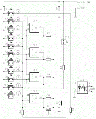
A different Electronic Security Door Key Circuit Diagram of electronic lock very simple, one and does not need a lot of materials in order to it is manufactured. The right keys of code should be stepped with the right line, so that is activated the optocupler IC2. If from error is stepped switch that does not belong in the combination, then the lock is trapped. In order to we restore the regular operation of lock, it should we press switches S1 or S12. 

Read : Heat Detector Alarm using UM3561 

 Electronic Security Door Key Circuit Diagram

Electronic Security Door Key Circuit Diagram


Switch S1 makes Reset of lock externally and the S12 internally, the door. The Code the circuit as he is connected it is 147 and it can change, very easily, changing the connections in the switches of keyboard. The optocupler IC2, can drive any exterior circuit as Relay etc, ensuring simultaneously electric isolation the two circuits. The circuit can be also supplied from a battery 9V.

Read : Radio Wave Alarm

Part List

    R1-7-9=1Kohm
    R2-3-4-5=100Kohm
    R6 =10Kohm
    R9 =47Kohm
    IC1 = 4066
    IC2 =4N25
    Q1-2=BC550
    S1...11=Push button sw or keyboard
    S12=Push button normal closed
    All resistors is 1/4W 5%
Readmore...

Wednesday, August 13, 2014

Voltage Converter 0 5v to 6v Circuit Diagram

This is a Simple Voltage Converter 0.5v to 6v Circuit Diagram. Conventional silicon transistors just cant operate at voltages less than about 0.7v. Old germanium transistors could be used, but those are hard to find these days and most are rather large in size. Some new n-channel MOSFET devices with very low gate-source threshold voltage can operate at quite low voltages. Ive been experimenting with various devices and came up with one electronic circuit (shown below), which demonstrates how to boost the low voltage from a single solar cell to a higher voltage. 

Voltage Converter 0.5v to 6v Circuit Diagram

Simple Voltage Converter 0.5v to 6v Circuit Diagram


The key component in the circuit below is a cheap single logic device from Texas Instruments. It turns out that TIs 74AUC family of parts can work down to about 0.45 volts. I tried one of their single schmitt trigger parts and found I was able to make on oscillator function nicely at 0.5 volts. I then used a charge pump technique and a cheap NPN transistor to form a low power flyback converter. 

This hobby circuit can produce about 6 volts at the output from a 0.5v input. The idea is to use this boost circuit to generate the higher starting voltage needed by a much more powerful DC to DC converter. Once started, part of the converters output could then be feed back to the input, to sustain converter operation. This is known as a "bootstrap" technique. In the future, I hope to post a circuit which can supply several watts of power from a 0.5v input voltage. This would be ideal for charging a battery using power from a single large solar cell or several smaller cells wired in parallel.


Drown By : Dave Jhonson
Readmore...

Saturday, January 11, 2014

Dual Regulated Power Supply Circuit Diagram

In this circuit, the 7815 regulatates the positive supply, and the 7915 regulates the negative supply. The transformer should have a primary rating of 240/220 volts for europe, or 120 volts for North America. The centre tapped secondary coil should be rated about 18 volts at 1 amp or higher, allowing for losses in the regulator. An application for this type of circuit would be for a small regulated bench power supply. 

 Dual Regulated Power Supply Circuit Diagram

Dual Regulated Power Supply Circuit Diagram

Readmore...

Friday, January 10, 2014

Low Power Voltage Reference Circuit Diagram

The Low Power Voltage Reference Circuit Diagram described below, is a special implementation of current source LM334. Characterized by a very small temperature coefficient metatholio output voltage and consumes only 10uA room temperature. This current fluctuates by a few uA, when the ambient temperature varies significantly. The positive rate of temperature change LM334 offset by the negative of the contact base emitter transistors has a direct thermal coupling with the integrated. 

To achieve the lowest possible temperature coefficient, it is necessary to adjust the output voltage of 1,253 V source to the arrangement easily done through R1. From the moment you get the desired output voltage, you are advised to stuck P1 and after the count value, replace it with a constant resistance. The best indeed is to replace P1 with the R1, so you have fewer parts. Prefer metal film resistors and tolerance of 1% E96 series. Having as a given that the output voltage obtained from the pin configuration LM334, is expected to show a negative resistance value 3.8 KO. 

The resistance A3 ensures that the output impedance will be equal to 400 W. Under these conditions, the current that can provide the source to the load to be connected to out of retained less than 5 Ma stability of the voltage source is more than satisfactory. By varying the input voltage from 5 V to 30 V, the change in output was only 0.6 mem (from 1.2530 to 1,2536 V). The change in the thermal coefficient is maintained at values ??less than 50 ppm / C, and if you worry a bit more to the setting of the circuit, you will see that quite easily reaches 5 ppm / C. The requirements of the original circuit current was only 9.8 mA at a temperature of 22C.

Low Power Voltage Reference Circuit Diagram

Low Power Voltage Reference Circuit Diagram

Readmore...

Thursday, January 9, 2014

Simple 15V And 5V Car Battery Supply Circuit Diagram
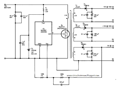
This is a Simple 15V And 5V Car Battery Supply Circuit Diagram. In this circuit use IC1 is a switching regulator that generates a 45-kHz signal that drives the gate of MOSFET Ql. Dl, D2, and D3 are Schottky diodes. The 5-V output is sensed as a reference; feedback to the chip turns off the gate signal to Ql if the voltage rises above 5 V. 

Tl has Trifilar windings that assume about 2% regulation for a 10-to 100-mA load change on the ± 15-V supplies. R1/D4 provide over-voltage protection. Tl has a primary inductance of about 21 . Core size should allow 4-A peak currents. The turn ratios are IIV2 turns each for the 15-V supplies, ll1/2 turns for the primary, and four turns for the 5-V secondary. The efficiency is about 75%.

Simple 15V And 5V Car Battery Supply Circuit Diagram

Simple 15V And 5V Car Battery Supply Circuit Diagram

Readmore...

Friday, December 27, 2013

5 LED VU meter circuit diagram using KA2284

This is a simple circuit diagram of 5-LED audio VU meter using IC KA2284/KA2285. The KA2284, KA2285 are monolithic integrated circuit. It is a logarithmic display driver IC. And it is Bar type display driver using 5-Dot LED. The KA2284/KA2285 has a wide range supply voltage capacity of 3.5V-16V, but we recommend to use about a 12VDC power supply.

Circuit Diagram:


KA2284-led vu meter
Fig: 5-LED Dot/Bar (VU meter) circuit diagram

Usability of this circuit:

  • AC signal Meter or DC Level meter.
  • Audio VU(Volume Unit) meter in amplifier or such kind of device.
Here IC AN6884 is also can be used instead of KA2284,KA2285. These all are almost same.
Further reading: DOT vs BAR
Readmore...

Monday, December 23, 2013

3 Rail Power supply Circuit Diagram

This 3- Rail Power supply Circuit Diagram generates three supply voltages using a minimum of components. Diodes D2 and D3 perform full-wave rectification, alternately charging capacitor C2 on both halves of the ac cycle. On the other hand, diode D1 with capacitor C1, and diode D4 with capacitor C3 each perform half-wave rectification. 

The full-and half-wave rectification arrangement is satisfactory for modest supply currents drawn from -5 and +12-V regulators IC3 and IC2. You can use this circuit as an auxiliary supply in an up-based instrument, for example, and avoid the less attractive alternatives of buying a custom-wound transformer, building a more complex supply, or using a secondary winding, say 18 Vac, and wasting power in the 5-V regulators.

3- Rail Power supply Circuit Diagram

3- Rail Power supply Circuit Diagram

Readmore...

Sunday, December 22, 2013

Easy Dc To Dc Converter Circuit Diagram

This Easy Dc To Dc Converter Circuit Diagram uses a Linear Technology LT1073 in a -24-V converter. The supply can be two AA cells (3 V) or 5 V. The circuit can deliver 7 mA.


Dc To Dc Converter Circuit Diagram

Easy Dc To Dc Converter Circuit Diagram

Readmore...

1000 watt power inverter circuit diagram

This 1000 watt power inverter circuit diagram based on MOSFET RF50N06.If you want more power then  add additional  MOSFET paralleled at RF50N06.This MOSFETS are  60 Volts and 50 Amps as rated.  It is necessary to connect  a  FUSE with the power line and always a LOAD have to connected while power is being  applied . The output power of this inverter is up-to 1k watt , it depends on output power transformer . You can use your custom transformer with experimenting for best result.

Circuit Diagram | 1000 watt power inverter


1000w inverter circuit
Fig:Schematic diagram of 1000 watt power inverter

How to parallel MOSFETs | 1000 watt power inverter


parallel MOSFETs


Source: http://www3.telus.net/chemelec/Projects/Inverter/Mosfet-Inverter.htm
Readmore...

Friday, December 20, 2013

Warning Light and Marker Light Circuit Diagram

This is a Warning Light and Marker Light Circuit Diagram. A flashing light of high brightness and short duty cycle is often desired to provide maximum visibility and battery life. This necessitates using an output transistor, which can supply the cold filament surge current of the lamp while maintaining a low saturation voltage. The oscillation period and flash duration are determined in the feedback loop, while the use of a photo transistor sensor minimizes sensitivity variations. 


Warning Light and Marker Light Circuit Diagram

Warning Light and Marker Light Circuit Diagram
 
Readmore...

Monday, December 16, 2013

Simple Battery charger Circuit Diagram

This is a simple Battery charger circuit diagram. A diac is used in the gate circuit to provide work for the signal being applied to the gate. R1 a threshold level for firing the triac. C3 and R4 is selected to limit the maximum charging cur-provide a transient suppression network Rl, rent at full Totation of R2. R2, R3, Cl, and C2 provide a phase-shift net.


Simple Battery charger Circuit Diagram


Simple Battery charger Circuit Diagram
Readmore...

Tuesday, October 8, 2013

SOFT START MECHANISM FOR L200 VOLTAGE REGULATOR ELECTRONIC DIAGRAM

SOFT START MECHANISM FOR L200 VOLTAGE REGULATOR ELECTRONIC DIAGRAM

Ic (constant current) is charge capacitor C, where Ic = Vsc/R.

The output reaches its nominal value after the time ton. Vo-Vsc=(Ic.ton)/C.

ton=C.[(Vo-0.45)/0.45].R = CVoR/0.45.

Vo follows the voltage in pin 2 at less than 0.45 volt. It is because voltage of more than 0.45 V can’t be produced between pin 2 and pin 5.
Readmore...

Sunday, October 6, 2013

0 5 WATT MINI AMPLIFIER TDA1015T ELECTRONIC DIAGRAM

0,5 WATT MINI AMPLIFIER TDA1015T ELECTRONIC DIAGRAM

Chances are youll want this amplifier portable. Batteries do the trick fine, but you wont get much power out of a couple of 1.5V cells. Unfortunately the size of a decent amount of battery power will mean that the overall size of this amp will be much bigger and for that there are more benefits to be had using a device like the TDA7052 or TDA2822 for stereo.

Quick ref data of TDA1015T Chip

  •     Supply voltage range: 3,6 to 12 V
  •     Peak output current: 1 A
  •     Output power: 0,5 W
  •     Voltage gain power amplifier: 29 dB
  •     Voltage gain preamplifier: 23 dB
  •     Total quiescent current: 22 mA
  •     Operating ambient temperature range: -25 to +150 °C
  •     Storage temperature range: -55 to + 150 °C
Readmore...

Sunday, September 29, 2013

1967 69 Chevrolet Camaro Wirng Diagram

1967-69 Chevrolet Camaro Wirng Diagram
The Part of 1967-69 Chevrolet Camaro Wirng Diagram: battery, generator, clutch switch, ignition
switch, voltage regulator, starter relay, neutral safety sitch, black wire, blower motor, widhshield wiper motor, heater ctrl light, radio illumination light, dome light, headlight switch
Readmore...

2002 Chevrolet Chevy Impala Wiring Diagram

2002 Chevrolet Chevy Impala Wiring Diagram


The Part of 2002 Chevrolet Chevy Impala Wiring Diagram: power distribution, battery, ignition switch,
junction block, crank relay, starter solenoid, relay ctrl, powertrain ctrl module, crank voltage, fusible link, generator,black wire,  solenoid contacts, yellow wire, schematics
Readmore...

Saturday, September 28, 2013

1995 Buick Park Avenue Wiring Diagram

1995 Buick Park Avenue Wiring Diagram

The Part of 1995 Buick Park Avenue Wiring Diagram : cornering lamps, turn flasher, power distribution, relay center, fuse block, yellow wire, assembly, see ground, green wire,
Readmore...

Thursday, September 26, 2013

ALTERNATING FLASHER ELECTRONIC DIAGRAM


ALTERNATING FLASHER ELECTRONIC DIAGRAM

The first IC used as a 1 second clock, which generates ON/OFF for the other ICs. Diodes help to cover the IC555 from the peak voltage. Take note that the relay used should have impedance more than 50 ohm.

Parts list :


  •     Diode D1-D2 : 1N4001
  •     Zener Diode D2 : 6V
  •     R1,R5,R7 : 3k3
  •     R2,R6,R8 : 68k
  •     Resistor variable VR1 : 47k
  •     Polar capacitor C1 : 10uF/16V
  •     Polar capacitor C3,C5 : 2.2 uF/16V
  •     Capacitor C2,C4,C6 : 0.01 uF
  •     Transistor T1 : BC107/BC148
  •     IC timer : NE555
  •     Relay : 6-9 V
  •     Power supply 6-9 V


Readmore...

Wednesday, September 25, 2013

1983 Ford Bronco Wiring Diagram

1983 Ford Bronco Wiring Diagram

The Part of 1983 Ford Bronco Wiring Diagram: blower motor, coolant temp, ignition module, select
switch, resistance wire, horn relay, alternator, relay, stop light switch, fuse box, directional flasher, low brake, hazard flasher, coolant temp switch, high beam, fuel gauge, license lights, red wire, tail light, instrument light

Readmore...

Monday, September 23, 2013

MOSQUITO REPELLENT ELECTRONIC CIRCUIT DIAGRAM

MOSQUITO REPELLENT ELECTRONIC CIRCUIT DIAGRAM

It uses IC CD4047 to control the buzzer timing utilizing resistor and capacitor. When the voltage passing through the transistor, the buzzer would sound.

    Variable resistor R1 : 10K ohm
    Polar capacitor C2 : 4.7 nF/16V
    Capacitor C3 : 22uF
    IC1 : CD4047
    NPN transistor Q1-Q2 BC547
    PNP transistor Q3-Q4 BC557
    Buzzer K1 : Tweeter 8 ohm
    Power supply : 12V
Readmore...

Sunday, September 22, 2013

USB Powered Audio Power Amplifier Circuit Diagram

This circuit of multimedia speakers for PCs has single-chip-based design, low-voltage power supply, compatibility with USB power, easy heat-sinking, low cost, high flexibility and wide temperature tolerance. At the heart of the circuit is IC TDA2822M. This IC is, in fact, mono-lithic type in 8-lead mini DIP package. It is intended for use as a dual audio power amplifier in battery-powered sound players. Specifications of TDA2822M are low quiescent current, low crossover distortion, supply voltage down to 1.8 volts and minimum output power of around 450 mW/channel with 4-ohm loudspeaker at 5V DC supply input.

An ideal power amplifier can be simply defined as a circuit that can deliver audio power into external loads without generating significant signal distortion and without consuming excessive quiescent current. This circuit is powered by 5V DC supply available from the USB port of the PC. When power switch S1 is flipped to ‘on’ position, 5V power supply is extended to the circuit and power-indicator red LED1 lights up instantly. Resistor R1 is a current surge limiter and capacitors C1 and C4 act as buffers. Working of the circuit is simple. Audio signals from the PC audio socket/headphone socket are fed to the amplifier circuit through components R2 and C2 (left channel), and R3 and C3 (right channel).

Circuit diagram:

USB Powered Audio Power Amplifier Circuit Diagram

USB Powered Audio Power Amplifier Circuit Diagram

Potmeter VR1 works as the volume controller for left (L) channel and potmeter VR2 works for right (R) channel. Pin 7 of TDA2822M receives the left-channel sound signals and pin 6 receives the right-channel signals through VR1 and VR2, respectively. Ampl i f ied signals for driving the left and right loudspeakers are available at pins 1 and 3 of IC1, respectively. Components R5 and C8, and R6 and C10 form the traditional zobel network. Assemble the circuit on a medium-size, general-purpose PCB and enclose in a suitable cabinet. It is advisable to use a socket for IC TDA2822M. The external connections should be made using suitably screened wires for better result.

Author: T.K. Hareendran - Copyright: EFY Mag

Readmore...