Showing posts with label driver. Show all posts
Showing posts with label driver. Show all posts
Wednesday, September 4, 2013
6 Channel LED Driver Using MCP34845
A very simple 6 channel low cost led driver electronic circuit project can be designed using the MCP34845 LED drivers manufactured by Free scale Semiconductor.The MCP34845 LED drivers operates from 5 to 21 volts and is specially designed for use in back lighting LCD displays from 10" to 17"+ for devices like : PC Notebooks , Net books , Picture Frames , Portable DVD Players , Small Screen Televisions , Industrial Displays , Medical Displays , etc.
6 Channel LED Driver Circuit Diagram
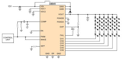
The MCP34845 LED drivers is capable of driving up to 16 LEDs in series in 6 separate strings.PWM dimming is performed by applying a PWM input signal to the PWM pin which modulates the LED channels directly.Main features of this driver circuit project are : input voltage of 5.0 to 21 V , boost output voltage up to 60 V, 2.0 A integrated boost FET , fixed boost frequency - 600 kHz or 1.2 MHz , OTP, OCP, UVLO fault detection , LED short/open protection , programmable LED current between 3.0 mA and 30 mA .
6 Channel LED Driver Circuit Diagram
The MCP34845 LED drivers is capable of driving up to 16 LEDs in series in 6 separate strings.PWM dimming is performed by applying a PWM input signal to the PWM pin which modulates the LED channels directly.Main features of this driver circuit project are : input voltage of 5.0 to 21 V , boost output voltage up to 60 V, 2.0 A integrated boost FET , fixed boost frequency - 600 kHz or 1.2 MHz , OTP, OCP, UVLO fault detection , LED short/open protection , programmable LED current between 3.0 mA and 30 mA .

Tuesday, September 3, 2013
4A High Speed Low Side Gate Driver
The UCC27518 and UCC27519 single-channel, high-speed, low-side gate driver device is capable of effectively driving MOSFET and IGBT power switches. Using a design that inherently minimizes shoot-through current, UCC27518 and UCC27519 are capable of sourcing and sinking high, peak-current pulses into capacitive loads offering rail-to-rail drive capability and extremely small propagation delay typically 17 ns.
The UCC27518 and UCC27519 provide 4-A source, 4-A sink (symmetrical drive) peak-drive current capability at VDD = 12 V. The UCC27518 and UCC27519 are designed to operate over a wide VDD range of 4.5 V to 18 V and wide temperature range of -40°C to 140°C. Internal Under Voltage Lockout (UVLO) circuitry on VDD pin holds output low outside VDD operating range.
4A High-Speed Low-Side Gate Driver Circuit diagram:

Features:
Device Uses:
The UCC27518 and UCC27519 provide 4-A source, 4-A sink (symmetrical drive) peak-drive current capability at VDD = 12 V. The UCC27518 and UCC27519 are designed to operate over a wide VDD range of 4.5 V to 18 V and wide temperature range of -40°C to 140°C. Internal Under Voltage Lockout (UVLO) circuitry on VDD pin holds output low outside VDD operating range.
4A High-Speed Low-Side Gate Driver Circuit diagram:

Features:
- Low-Cost, Gate-Driver Device Offering Superior Replacement of NPN and PNP Discrete Solutions
- Pin-to-Pin Compatible With TI’s TPS2828 and the TPS2829
- 4-A Peak Source and 4-A Peak Sink Symmetrical Drive
- Fast Propagation Delays (17-ns typical)
- Fast Rise and Fall Times (8-ns and 7-ns typical)
- 4.5-V to 18-V Single Supply Range
- Outputs Held Low During VDD UVLO (ensures glitch free operation at power-up and power-down)
- CMOS Input Logic Threshold (function of supply voltage with hysteresis)
- Hysteretic Logic Thresholds for High Noise Immunity
- EN Pin for Enable Function (allowed to be no connect)
- Output Held Low when Input Pins are Floating
- Input Pin Absolute Maximum Voltage Levels Not Restricted by VDD Pin Bias Supply Voltage
- Operating Temperature Range of -40°C to 140°C
- 5-Pin DBV Package (SOT-23)
Device Uses:
- Switch-Mode Power Supplies
- DC-to-DC Converters
- Companion Gate Driver Devices for Digital Power Controllers
- Solar Power, Motor Control, UPS
- Gate Driver for Emerging Wide Band-Gap Power Devices (such as GaN)
Subscribe to:
Posts (Atom)